About EV CHARGER PCB ASSEMBLY
- PCB Assemblies (RHS, Leaded) with highest Quality and on-time delivery
- Focus on Engineering prototypes and Low-mid Volume manufacturing with Quick turnaround time
- Supports Single sided, Double sided, surface mount and through-hole Assembly
- Assembly of Rigid, Semi, Rigid and Flex PCB
- Machine and manual soldering Options
- Meticulous assembly backed by highly skilled professionals and process
- Comprehensive & multi-stage QC process ensures consistent quality and high production
- Emphasis on material / Kit verification to minimize in-process delays, rejects & reworks
- Quality control test equipments backed by a highly skilled test engineering team
- Development of Customer specific Test jig
- Hot-lot Assembly services for Urgent Requirements using reserved resources. Pick and delivery support to improve turnaround time
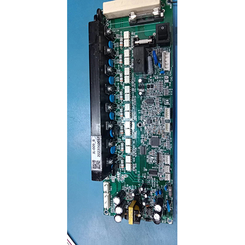
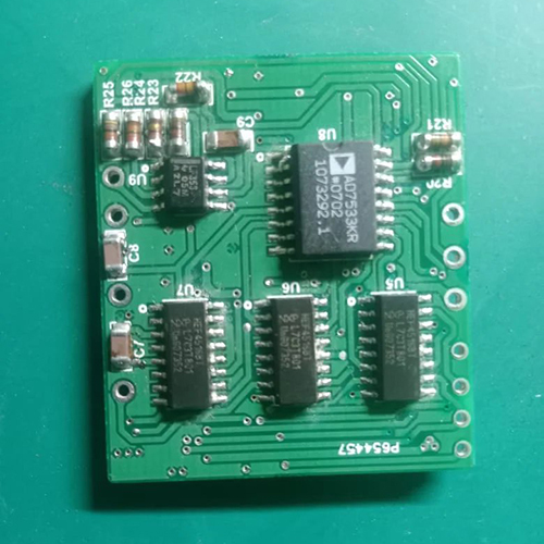
Reliable Multi-Layer ConstructionThis 4-layer PCB assembly is built from high-grade FR4 materials, providing structural stability and durability. The 1.6 mm thickness alongside 35 m copper layers ensures robust electrical performance and makes it an ideal foundation for electric vehicle charging infrastructure. The green solder mask offers extra protection against environmental impacts.
Advanced Communication and ControlSupporting versatile communication protocols including CAN, UART, and RS485, this charger PCB allows seamless integration with various control and monitoring systems. Firmware remains future-ready with upgradability via USB, enabling adaptability for evolving EV standards and station requirements.
Optimized for Safety and EfficiencyEquipped with advanced protection features - overcurrent, overvoltage, and short circuit safeguarding - your charging stations remain secure. The optimized thermal via design ensures efficient heat dissipation, enhancing device longevity and supporting a life cycle exceeding 100,000 cycles.
FAQ's of EV CHARGER PCB ASSEMBLY:
Q: How does the thermal via design improve heat dissipation in this EV Charger PCB Assembly?
A: The PCB incorporates a thermal via design, which efficiently transfers heat away from sensitive components, preventing overheating and enhancing the overall reliability and life span of the assembly during extended operation.
Q: What communication protocols are supported, and how does this benefit electric vehicle charging stations?
A: The assembly supports CAN, UART, and RS485 protocols, allowing flexible integration into various EV charging networks. This compatibility ensures smooth data exchange and interoperability with different charging infrastructure and remote monitoring systems.
Q: When is firmware upgraded, and what is the process for updating it?
A: Firmware upgrades are performed conveniently via the onboard USB port whenever new features, improvements, or security patches are available. This ensures that the charger remains compatible with the latest standards without complex procedures.
Q: Where can this EV Charger PCB Assembly be used, and what are its primary applications?
A: This PCB assembly is designed for electric vehicle charging stations, making it suitable for both public and private EV charging points across India and globally, wherever reliable DC charging control is needed.
Q: What protection features are included to ensure safe operation?
A: The assembly is equipped with overcurrent, overvoltage, and short circuit protection, safeguarding both the charger and connected electric vehicles from electrical faults or anomalies.
Q: How does this product comply with environmental and safety standards?
A: The EV Charger PCB Assembly is RoHS compliant, meaning it is manufactured without hazardous substances, contributing to environmental safety and sustainability.
Q: What is the expected life cycle of this PCB assembly, and what are the benefits for long-term usage?
A: Boasting a life cycle greater than 100,000 cycles, this assembly is ideal for high-usage environments, significantly reducing maintenance and replacement costs for charging station operators.
 Send Inquiry


 Send Inquiry
